Showing posts with label PWM. Show all posts

Tuesday, August 28, 2012

PWM amplifier 1 - The PWM modulator design III.

On my previous analysis, I didn't pleased with the quality of triangle signal, but a little modification made better result. In the second article, the triangle (and the PWM) signal is better, but not perfect. This is the reason why I simulated the modulator design with another oscillator circuit.


The design is very simple, simplest then the previous signal generator version. This new contains simple CMOS oscillator. The design is small, simple, and the output signal is perfect. The duty-cycle is always 50%, the amplitude of square signal is 5...15V if required. The frequency setting is very easy, on 10 MHz the square signal is really nice.

The red is the square output of CMOS circuit, the green is the triangle signal.

The triangle and the square signal is much better compared to the analog oscillator circuit.

This is the schematic, the difference between R1 and R2 is 10x, the capacitor can be very small value, the frequency is very stable.
Unfortunately, the upper ideal stage will be wrong if I continues the design with comparator circuit on the simulation. (See the schematic, I did not continued the triangle output to the comparator input). If the triangle signal after CMOS (or TTL) circuit wired to the comparator, the signal will be non-usable:
The square signal stay good, but the triangle signal going wrong on the simulation.

 The usefulness triangle signal.

I did nothing else, I just continued the signal with comparator.

The upper problem can be solved with a small modification, see the images and the power source of the comparator on the schematic:


On the circuit, I using independent DC power source for comparator chip only. After I getting back the nice signals, but with this design the comparator doesn't made PWM signal from sources. If I used common ground, the comparator started to work, but the triangle (and the PWM) signal is going wrong again:

Transient analysis result when the CMOS oscillator and the comparator have common ground:

At this moment I don't know how to solve the problem on the simulator. I wonder, (and not sure) about the result of real circuit. The simulation is usefulness, but the oscillator design is better and simpler before using comparator. So at this moment, the analog oscillator design is much better than this new one.

PWM amplifier 1 - The PWM modulator design II.

I have successfully cleared the last design example of PWM modulator circuit. This PWM modulator will be used before TAS H-bridge chip. In this article, I don't really like the signal at the end, and I made mistakes about power sources (with Zener diodes) on the last simulation schematic. Not too much, but I modified the design, and I got better result. I deleted the dead-time logic, because for the TAS chip not required, the soft start only is easier. At the end of this newer design, I got nice signal from both TTL and CMOS outputs and comparator without dead-time logic. See images.

In this image the green is the triangle signal, the red is 10 kHz sinus, a yellow is the PWM output on the CMOS 4009 inverter.

I know, that not really important, but how I know about the quality of modulated PWM signal? I have to convert back to the original with RLC network. This is the blue line.
I changed the CMOS 4009 (15V power for comparator and CMOS circuit) to TTL 7414 (5V power for comparator and TTL circuit). The TTL output is the yellow line.

 The decoded result at the end of TTL circuit is the blue signal.

I made small modifications on the circuit around the comparator. I changed Z diodes DC power sources, the output of the comprator continued with only one TTL or CMOS gate (inverter). I analyzed the PWM signal after the TTL/CMOS chip, but the output of comparator is really good too with this schematic:

Friday, August 17, 2012

PWM amplifier 1 - The PWM modulator design I.

Newly detected TAS5630 chip can solve my problems about the PWM amplifier. This chip have analog inputs, the package contains all required parts (A/D converter, PWM modulator), and the parallel mode is possible if less than 4 Ohm output impedance required. with this package we have one paralleled mono or one stereo poweramp with analog input.

But I have TAS5261 chips, without analog input. For this design required TAS55xx PWM modulators and analog/digital converters. These chips recommended for home DVD  players, the power supply is 3.3 volts only. I don't think that this solution is ideal for instrument amplification.

In this post, I writing about the method and simulation of analog PWM modulator.

First I need a triangle function generator. I found too much... The clock of PWM input TAS chip is 192-384 kHz, what is understandable if digital chips placed before chip. For this frequency, not too easy to find triangle signal generator with very good output.

Can be found one-chip function generators. One of them is LM566 (with this chip I found a schematic) not available here and now, or we can use XR2206 or ICL8038 chips. These chips are very simple solutions for triangle output, maybe I will try some of them. The maximum frequency on the datasheet is 0.5MHz, typical is 1MHz, but the 8038 have 300kHz maximum. I have no experiences with these function generator chips, so I don't know about the output quality. This is the reason, why I seek discreet analog function generator for triangle output. The another reason, is, function generator chips are not available on Multisim.


The first tryouts I have no success:
This function generator promised for perfect output, but the triangle with 20 kHz only is really bad. So I don't need to try this design for 200-300 kHz.

I tried more triangle generators with op-amps, but the output is not good enough. Finally I found a really good analog triangle generator with nice triangle and square outputs. This circuit can be used up to 4MHz what is more than enough.

I have good result on 300kHz:
See the simulation output, this is 235 kHz. Very easy to set the frequency and duty cycle.

I tested this discreet (but easy to set) schematic  on higher frequency. Here ate the test results:

1.3 MHz:
2MHz:
3.5 MHz:
6 MHz:

I think, if the upper schematic is good enough on 2-4 MHz, then this is good for around 300 kHz only.

The triangle output of this circuit wired to the fast comparator. the most of comparators doesn't worked on Multisim for me, but finally I found one what is very good for output simulation:
 
Example about the signals in the circuit:
The purple line is the triangle output of function generator, the green is the part of 1kHz sinus (audio) input, the red is the TTL PWM modulated square with variable duty cycle.
In this image can be seen how duty cycle modulated by the sinus input signal:

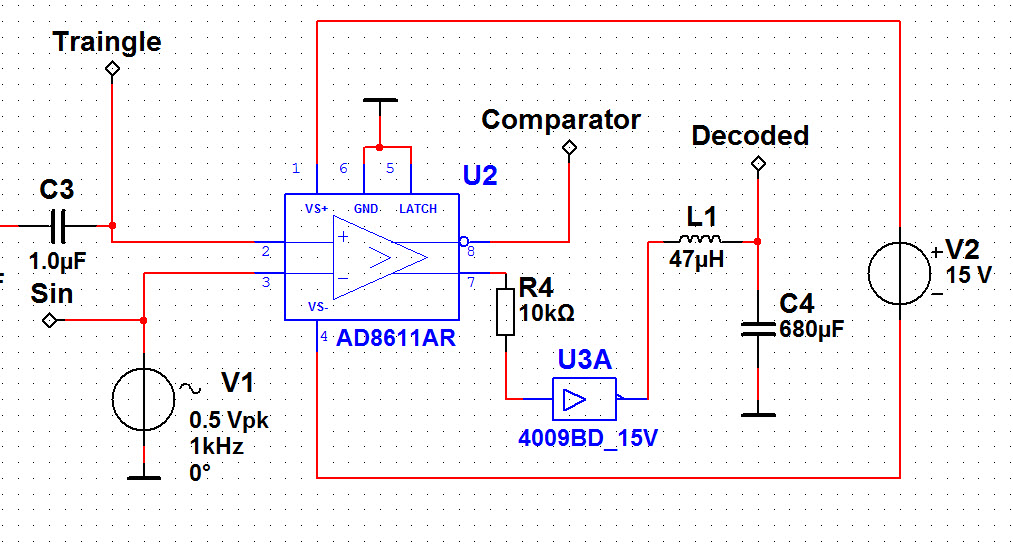
Continued the circuit simulation, the next is the comparator. This part AD8611 is good on Multisim, but I think another comparator (for example LM311) is good on real life too. The triangle signal and the audio (sinus) input have to be connected to the comparator's inputs.


The most important question is, the quality of the PWM modulated output. What I get back, if the PWM modulated square signal converted back to the original sinus wave. The quality of this method cannot seen by the quality of the PWM modulated output. See the image:

The green line is the original audio sine wave signal. I have to get back this wave from the PWM outputs. The dark-red is the (good) result if the PWM output converted back to the original sine. What is the blue line, I will tell you soon....

After the comparator chip, I put TTL logic. This logic made soft start while the triangle generator up, and disabled the input of TAS H-bridge. This method made inverted and non-inverted PWM outputs. Finally this is the "deat time" logic. The TAS5261 contains "dead time" logic, and the most if comparators have inverted and non-inverted outputs. This TTL logic required, if the output of PWM amplifier is simple MOSFETs, not H-bridge chips with internal logic what I want to use.

......the blue line (what is really wrong and distorted) is the converted output of TTL chips.
Here are the signals in this design: The sine is 20 kHz now, the blue line is the triangle signal on 235 kHz, the red line is the TTL PWM output, the tall brown line is the output of comparator. The result is much better on the comparator output.


After simulation results I have many problems.

The first question is about the precision of simulation. How about the simulation and the  reality, whats about the differences, depending on the PCB design and the quality of parts.
After these PWM modulated square waves, I have to put TAS H-bridhe chips, and I can use these outputs for audio. Maybe this method have good result, but maybe not. Maybe the TTL outputs (what is really wrong after decoding on the simulation result) good enough for discreet MOSFET drivers. Finally I have to test the DC offset of comparator inputs and outputs, and the linear frequency range of the decoded output. These solutions is on the next post.

Tuesday, July 24, 2012

New PWM power chips with analog inputs

In the previous article I thinking about the poweramps of my guitar/vocal amplifier. The power supply is ready, I have 1200VA, this is the reason why I want to include more than one guitar amp to this new design. But whats about the top of this amplifier case, where I need poweramps and preamps?

I think for the guitar amp I will use bridged TDA7293 because for 8 or 16 Ohm speakers the bridged amp solution is better. But for keyboard/vocal I wanted to use Class-D TAS chips. These chips have 125W output power for 8 Ohm, but 315W for 4 Ohm. The impedance of additional cabinet for vocal or for guitar can be 4 Ohm (or less) if required. In my previous DIY amplifier I used bridged TDA chips, and I really like it. This is the reason why I want "hybrid" solution. One analog amplifier for guitar with TDA chips, and another one for all others with PWM solution.


This is one example that the 4x200W TDA bridged solution is more than enough for clubs for guitar and vocal (but this is gym):


For the PWM solution I think about TAS5261 chips. This is small power bridge with PWM input, but PWM modulator and A/D converter required. I have no experience with these chips, and these solutions have very small size, I am not sure that I can assemble them.

This chip is 2x210W PWM power-bridge with the smaller package.

This is TAS5261 chip, 1x350W power bridge.

I like these solutions, error and speaker protections included, chips have very good efficiency, no large heatshink required. The efficiency of TDA solution is about 60%, but his PWM chip have more than 90%.

But these TAS chips offered for home theater or home DVD systems, maybe not for instrument amplification. See the datasheet:
  • 315W - 4 Ohm
  • 220W - 6 Ohm
  • 125W - 8 Ohm
This is the reason why I don't want to use this solution for 8 Ohm guitar speakers, but maybe want to use for 4 Ohm vocal or additional cabinets.


The another thing that I don't want to use required additional circuits like A/D converters and PWM modulators. These chips have very small package, and the power is 3.3V only.

The PWM modulator:

The one pin of this chip 0.2mm width, the distance between the middle line of pins are 0.5mm. Very hard to solder and assemble these parts.


But now the TAS PWM power bridges have analog inputs. PWM modulators and A/D converters not required. The package of these new solutions have 44 pin DKD, and the new 64 pin PHD. The 44 pin DKD package is same as like the previous TAS5261 chip. The biggest version of new analog input TAS chips have 600W power output, what is really great on very small size. See the datasheet page 18.

The benefits:
  • Very good efficiency (85...93%) no large heatshink (and cooler) required
  • Have analog inputs, no PWM modulators and A/D converters needed
  • The chip have error protection
But:

  • The 600W available on on 2 Ohm cabinet (the output of chips are paralleled)
  • 4 Ohm - 300W, what is not bad, but the previous chip have same feature.
  • 3 Ohm - 400W (paralleled outputs)
  • 6 Ohm - 210W
  • 8 Ohm - 160W.
But with these output powers have distortion 10% what is not small enough. If we need better quality, max. 1% distortion, the possible power will much smaller, the chip cannot be paralleled:
  • 4 Ohm - 240W. This is same as TDA bridged amplifier but on 8 Ohm impedance.
  • 6 Ohm - 160W
  • 8 Ohm - 125W
With smaller impedance with paralleled outputs on 1% distortion:
  • 3 Ohm - 310W
  • 2 Ohm - 480W
I found these solutions if I want to use PWM amplifier. The PWM chip is better than older solutions if I have speaker cabinet with 4 Ohm or less. I am not decided yet what will the poweramp on the top case of my guitar combo:


Wednesday, December 21, 2011

New PWM FAN controlers with speaker protection module

On the previous post I wrote about modular amplifier, can be connected to single, parallelled, and bridged mode (here is the PDF manual). The single amplifier is about 75-100W, bit with parallel and bridged mode the full poweramp maybe 700-800W (with bridged mode, but with 3 paralleled module). The original design contains one module for speaker protection with UPC1237 chip, which is very cheap and good solution. But the FAN controller for thermal protection is missing.

The thermal protection included to all TDA7293 chip, but no fan controller. The benefit of PWM FAN controller is the control sign is depend on the heatsink heat. I re-designed the PCB of speaker protection with PWM Fan controll circuit, but I made two versions. The first working with 4 OpAmps, and controls 3 fans with 10A output current:


The fan controller starts with 12V regulator, and the end of this circuit the 200V 10A MOSFET before fans. Paralleled with fans I have LED to display the "heat" of the system because the LED controlled with same same output like the fans.

Here is the PCB for this new module which compatible with the original speaker protection module:


This have PCB 7cm width, which is too much, so I looking for smaller and simpler fan controller circuit. Lot of solutions available on the NET with 555 and 556 timer IC, but I made something with MIC502 fan controller circuit. This circuit is simple and "vintage" DIL8 package, not the cheapest solution, but small, and not too much other parts required. The benefit of this solution, that the "sleep mode" setting. This is the threshold while the FANs not working (if not required).


with this simplest circuit I can design smaller PCB:


The width of this PCB is 55 mm instead of 70, what is good result. The speaker protection without PWM fan controller is 51 mm. This module now 4 mm wider.

I have one more choice to made PWM controller. The AMC6821 chip is really good solution. The chip made for computer mainboards, so the size is really small which is not really good for home designers, but maybe more smaller solution is good news for industrial designs.

The AMC6821 PWM Temp monitor and FAN controller chip:


The application of this is really easy and simple. The original module, contains speaker protection only is available if the single version of TDA729x modular amplifier required. But if using more modules for paralleled and bridged application, maybe for real instrument amplifications, the good heating system with temperature monitored FAN controller required.

See also:
PCB sales of this project
Module name Size
(mm)
Area
(cm2)
PDF SCH PCB image Tested Price (US$)
Des. Sim.1 Full2 Sim.1 Full2 Man3
PWM Fan controller V:1 70x57 40 Yes Yes Yes - - No 7
15 Ask
PWM Fan controller V:2 56x57 32 Yes Yes Yes - - No 6
14 Ask
How to order? Please read the rules carefully!