Tuesday, January 17, 2012

Modular, expandable parametric equalizer based on UREI546

I posted about the equalizer called UREI545 and UREI546. This is the one of my favorite project. These devices are not same, but very similar. The differences between 545 and 546, the LP/HP filter on the input, and the number of bands. On the original UREI545 have 3 parametric EQ filters, and one switchable filter with 3 different middle frequencies. The UREI546 have 4 bands without switchable frequencies, but this is dual device. Can be used as mono 8 band parametric EQ, or as 4 band stereo parametric EQ. These devices used by musicians for guitar and vocal equalization.

The current project based on the UREI546, but modified. The new design is an expandable parametric equalizer with modular system for smaller PCBs with no limitations. The maximum number of bands are not limited, but the current project made for 4 to 8 band equalizer, with optional input and output gain modules, optional HP/LP filter module, and optional clipping LED module. The design is similar as my previous modular expandable audio mixer or modular amplifier. The current project started with software simulation of filter circuit, and continued to get capacitor values for 8 band EQ by simulation. This is the post where I publish the schematic and PCB design of expandable modular parametric equalizer.

For the expandable feature, 2 mainboards required for this project. The first is for 4 modules, contains connectors for inputs (Conn2), outputs (Conn3), and +/-15V power supply (Conn1). This mainboard designed for 4 band EQ only, without additional modules:

Because between EQ modules and other modules requires serial connection, (not parallel like in the modular audio mixer), the last module on the whole system must be connected to the output bus. This is the reason why W1 and W2 jumpers are required. With these jumpers, the last module must be wired to the system output, without jumpers, the output of module connecting to the input of next module. The jumper must be used only on the last EQ or Output Gain module of the whole system. The connector P2 is 10 pin female connector, the next mainboard must be connected here if required. Conn4....Conn7 is 2x6 L headers for the EQ or Gain modules.

The PCB of first mainboard:


The second mainboard is more simple, contains only one 2x6 L header for one module, on the left one 10 pin male connector, on the right one 10 pin female connector:

W1 and W2 jumpers must used if the connected module is the last on the whole system. If last, the current module output connected to the system output bus by W1 and W2. The one and only exception, if the last module is the clipping detector. If more modules required, this mainboard must be connected to the previous one.

The PCB design:


The modules can be soldered to these two mainboards with 2x6 pins L header. The most important module is the parametric filter:

This filter based on UREI546 with some modifications. The Conn2 must be connected to the mainboard, the Conn1 is the connector for "power filter" module for less noise. This is the reason why the filter capacitor missing from the OpAmp. The C3 is coupling capacitor, 10uF or 22uF is better than 100nF in the original design. No need to change on several EQ modules. For EQ bands with different middle frequency, only 2 pieces of Ca capacitors must be changed. This is the reason, why the footprint accept 200 and 300 mil pins. Sw1 is the bypass switch, D2 diode is connected for the clipping detector bus. P1 adjust Q, P2 adjust the middle frequency, P3 adjust cut/boost of the EQ module.

The PCB:

The module cutted on the bottom because this required for mechanical assembly. The bypass switch and the 3 required potentiometers are soldered to the PCB. D1 is the connector for LED displays the bypassed or connected status of the module. The both mainboards made for stereo circuits, but this module (and currently all others) is mono. The reason of this difference, that in the future I would like to design stereo filters for stereo EQ, but I would like to use these mainboards. The lion in the way, that 4 potentiometers required to adjust the frequency if this EQ module going stereo.

The most important question about this module, the values of Ca (C1 and C2) capacitors. These values depend on the required middle frequency. I have no math expression, but I done software simulation for 8 bands with values.

  • Math expression required to get frequency values among the lowest and highest bands. This expression is used for Excel spreadsheet if the first and last frequency, and the number of other bands decided:
    =IF(C8<$D$5,$D$3*10^((LOG10($D$4)-LOG10($D$3))*(C8-1)/($D$5-1)), IF(C8=$D$5,$D$4,IF(C8>$D$5," ","?")))
  • The next is that we need the Ca capacitor value for the module frequency. This value is linear on the logarithmic scale with the frequency, but the best method is the software simulation. Here is an example for 8 band equalizer:

    The input of this spreadsheet is on the green fields on the top, contains the highest frequency of the first and last modules, and the number of all EQ modules. I always working with the highest frequency, the middle and the lowest value getting by the software simulation using modified standard capacitor values.
  • The real value of the module frequencies depend on the standard values of the capacitors. The best result is the software simulation again to getting the lowest and highest values of filters:
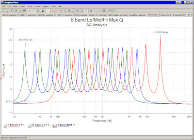
  • The number of possible requirements are very high. Not only the number of EQ bands, the lowest and highest frequency of the bands can be different. This is the reason, why I can publish and simulated 8 band EQ only. If you like another versions, for example less or more bands, or higher frequency of the lower band, software simulation required to get the capacitor values and the resistor values to setting Q.
The next module is a high pass/low pass filter circuit. I made little modifications compared to original one. About the LP/HP filter simulation see my next post. The current schematic with capacitor values:

With this design the bypass switch with LED, and the header for power filter are available too. The output connected to the clipping detector via D2, like all other filter modules. The C1 capacitor changed to 47pF to get better Q for higher frequency of LP filter. The potentiometers changed from 55kOhm to 22kOhm for smaller adjustment range. High adjustment range is not too important, because numerous adjustable filters can be connected after this module. The highest value of filter depend on C2 and C3 capacitor, what changed from 6.8nf to 4.7nF, but maybe 5.6 nF is the best because the new endpoint of frequency range is around 40kHz what is too much, but the original is around 15 kHz, what is low.

The capacitors of high pass filer is C4 and C5 changed to 470nF instead of the original 220nF to get lowest frequency. With this new value the filter starts from 15Hz, what is too low. Maybe 330nF would be the best, I will do simulation for several values soon.

The result of current AC analysis (470nF and 4.7nF):


The PCB of LP/HP filter module:


The next is a very simple and noiseless preamplifier module with jFET. I really like the sound of this circuit for guitar. This module can be used as first module (for input gain) and (or only) at the end of device as output gain:

This circuit can be bypassed by the switch, and can be ignored if not required.

The PCB:


The last module is the clipping detector what monitor all outputs of applied modules by the pin2 of 2x6 L header:


Clipping detector PCB:


The power filter, required for all modules for less noise except clipping detector:


I have 8 versions of power filter PCB where the difference is only the size of board. This is the version 6 with SMD resistors and transistors:


The required power supply and the PCB:


By these boards can be built like this (for example):

  • 4 bands mainboard, 4 pieces of EQ filters with the oroginal values of UREI546 can be the clone of original device but without preamplifier module, LP/HP filter, and clipping detector.
  • Start the whole device with 4 band mainboard, use the jFET gain module first, the second is the LP/HP filter module, and continue with 2 parametric EQ module. Connect mainboard 2 to mainboard 1, and use parametric EQ modules. When the maximum number of EQ modules connected, use one more jFET gain module for output gain (with W1 and W2 jumpers) and the last possible module is the clipping detector.

By software simulation the result of these circuits can be changed. The schematic samples on this post maybe set to wide values, but all modules adjustable, so I think this is not a big problem.

On the EQ modules and LP/HP filter modules maybe very important the logarithmic potentiometers. The resistor and capacitor values are linear, but with logarithmic scale of graph. On the simulation and on the schematic I used TL071...TL074, but for the best quality I offer using LT or NE series instead, what is much better for filter designs. For example for single OpAmp use LT1028/LT1128/LT1115, for quad or dual OpAmps can be changed to LT1124/LT1125.

See also:

PCB sales of this project
Module name Size
(mm)
Area
(cm2)
PDF SCH PCB image Tested Price (US$)
Des./3D Sim.1 Full2 Sim.1 Full2 Man3
4 band filter board V:1
88x55 48 - Yes Yes - - -
8
16 Ask
1 band filter board V:2 25x48
12 - Yes
Yes -
-
-
4 11 Ask
Parametric filter module
66x83 55
- Yes
Yes -
-
- 9 17 Ask
LP/HP filter module
66x63 42 - Yes
Yes
- -
- 7 15 Ask
I/O gain module
66x47 31 -
Yes
Yes -
- - 6 14 Ask
UREI clipping detector
22x34
7 - Yes
Yes
-
-
- 3 11 Ask
Power filter V:6 SMD
17x24
4 - Yes Yes - - -
3 11 Ask
Power supply
212x57 69 - Yes Yes
Yes - -
11 20 Ask
How to order? Please read the rules carefully!

Saturday, January 7, 2012

Simulation of 8 band parametric equalizer

On the previous post I talking about software simulation of parametric EQ filter. The simulation result is exactly same as the original official datasheet of 4 band EQ (with really small differences on the lowest frequencies). But I would like to design parametric EQ with more than 4 bands. No math expression, but the simulation is easier solution for this modification.

For the first design, I modified the original 4 band schematic to 8 bands, and the simulation works with this modification very fast, the required time is same as like with 1 filter only (while several software running on the background). The schematic simplified, I removed virtual batteries, used VCC/VEE power sources instead. Deleted the on/off switch which is really needless. This simplified schematic without virtual instruments working well for AC analysis.

First of all, I need math expression (again :) for getting frequency values between 20 Hz and 20 kHz for 8 bands. I think about 10 bands, but for parametric EQ where the middle frequency and the Q are adjustable, I think 10 bands are too much. The parametric EQ of URS software have 5 bands only. The first solution to get middle values between the lowest and highest band I found on the NET by this page. This webpage counts the geometric mean between f1 and f2, which are the lowest and highest frequencies on the system.

This solution is not the best for 8 bands, because first I can get the middle of the lowest and highest value which are 3 bands, but after, I have to get all middles between these 3 values, finally I have 5 or 9 results instead of 8. Maybe the possible solution if the highest frequency is around 40 kHz, get 9 results with this page, and delete the last (40 kHz) value. So you can have 8 results, where the highest around 20 kHz.

The really tricksy solution is the Excel spreadsheet. This table is not my own work, I got help from Frank Walker. I just enter the start and end values to this spreadsheet, and the required numbers between these values, and the table getting back the solutions.

First, compare the result of this expression with the original 4 band UREI EQ:


Compared with the UREI datasheet and the result of simulation, we can see, the datasheet values contains the result of expression not the simulation. The trust, on the UREI schematic I can found capacitor with 27.5 nf value, which is not the standard value.


Tables for more than 4 bands:

Finally, here is the expression of spreadsheet from the cell where we got the results of bands:
=IF(C8<$D$5,$D$3*10^((LOG10($D$4)-LOG10($D$3))*(C8-1)/($D$5-1)), IF(C8=$D$5,$D$4,IF(C8>$D$5," ","?")))

This expression counts the required frequencies between the lowest and highest bands. The lowest frequency is on the cell no. D3, the highest on D4, the number of bands is on the D5. The column C is the serial number of bands from 1 to 8.

More than 8 channels have problem with Q, what must be very high if the number of bands are too much. If less than 8 band required, all channels have bypass switch and the Q parameter can be set to lower.

For the current design, I need the table of 8 bands EQ. The range of frequency adjustment must be smaller than with 4 bands only, modifications of the schematic required:


The important aspect, that we have to work with standard values of capacitors and potentiometers. The first modification requires for possible higher Q value, and less possible range of the adjustment of Q:

  • R2 120 Ohm instead of 390 Ohm
  • R3 1.5 KOhm instead of 390 Ohm

The second modification is for the less range of frequency adjustment.

  • R5 and R7 potentiometers changed from 55 KOhm to 22 KOhm.

After these changes, on the filters have to be modified the C1 and C2 capacitors only:

  1. 330 nF
  2. 150 nF
  3. 68 nF
  4. 33 nF
  5. 15 nF
  6. 7.5 nF
  7. 3.6 nF
  8. C1 = 1.8 nF, C2 = 1.6 nF

Possible to fine tune the required frequency, if the values of C1 and C2 are not same. With this method, the required frequency can be fine shifted to lower or higher value, and can be re-tuned the value of Q.

First, I determine the maximum possible frequency (green) of the first (lowest) band by new C1 and C2 capacitors, and after I analyzed the low (red) and the middle (blue) frequency:

After analyzing the first band I started to define the second, but before, I wonder how about these bands on the original 4 band EQ:

This is the result of analysis for all 4 bands, with possible lowest, middle, and the possible highest frequencies.

Finally, the graph of AC analysis of 1st, 2nd, and 3rd frequencies not succeed pretty like on the original UREI EQ, because with available standard values this is not possible:

These graphs are not really pretty, but this is no problem, because the parameters are adjustable, and the graph cannot visible during operation :).

The next step is the AC analysis of all 8 bands:


The graphs are really not nice like the original one :(.

With the next analysis I reduced the Q from 100% to 70% on all bands:

This analysis would be more interested, if I bypass some filters, or changing the cut/boost parameter too.

Finally I tried to correct the "errors" of the graph. I reduced the bands frequency to 93...95% from 100, this is the thinner red line. The new line is closer to the green, which is the possible lowest frequencies of all 8 bands:

For this equalizer I have PCB for 4 and 6 bands only, but my next PCB project is the expandable modular parametric equalizer from 4 bands to any.

The available mainboard for 6 band parametric EQ:

See also:


PCB sales of this project
Module name Size
(mm)
Area
(cm2)
PDF SCH PCB image Tested Price (US$)
Des./3D Sim.1 Full2 Sim.1 Full2 Man3
Mainboard for 6 band EQ
173x143 247 - Yes Yes - - No 35
44 Ask
How to order? Please read the rules carefully!

Friday, January 6, 2012

Simulation and software analysis of UREI 546

This is my first post about simulation. The reason why I simulated UREI EQ filter, that I cannot found math expression to get parts for more than 4 bands parametric EQ, and I cannot modify the center frequency of original bands.

Finally I did software simulation, what is succeed. The simulation of analog circuits are very fast and exact, very easy to measure and analyze any parameters depending on the parts, easy to get result of parts modifications by graph or by simulated measuring devices. The best is, lot of AC sources and measuring instruments are available, like function generators and oscilloscopes. I used Multisim, because the simulation of Altium is more harder, and I cannot found good examples on the net how to use Altium for simulation. But as I see, the Multisim is very popular (because easy to use, I think):


This is the schematic of one filter from the UREI 546 parametric EQ. Function generator, one channel (yelow) of oscilloscope, and U3 AC voltmeter connected to the input. Second channel of oscilloscope (blue) and U2 AC voltmeter connected to the output. The power supply is the simulation of 2x18V DC power source. On/off switch, and bypass switch included. With simulation, all switches and potentiometers are working well and real time. To see the simulation result, the circuit is very exact, same as like datasheet of original UREI device, with really small differences. The bypass switch or the Cut/Boost potentiometer on center make the output voltage to same with input. I made a movie about simulation:


I wonder, the simulation result is same as the original datasheet, or have some differences. If the result is closed to the original datasheet, I don't need expression for the modifications.

I made new schematic with simple AC voltage source instead of function generator, and I deleted the scope from the output. I used AC analysis on the output point instead of scope. The result is more useful on the graph:


Here is the frequency response of the filter. All modifications can be analyzed and displayed with graph, for example new middle frequency, Q, and Cut/Boost function of EQ between 20 Hz and 20 kHz. Later I analyzed the circuit up to 100 kHz.

With these simulations, I can't compare the results with the original datasheet. Therefore I made 4 bands with exactly same values with the original schematic. I made AC analysis with min, max, and middle frequencies of 4 bands, and compared the maximum and minimum points to the official datasheet:


The red line is the lowest frequency on all 4 bands, the blue is the another side of potentiometer, the possible highest frequency. This is the comparison with the original EQ, where is the upper frequencies are really same, the lower shows small differences. Now I think, because the simulation result and the datasheet are same with small differences, the simulation of this schematic is good idea to modify the original EQ (instead of math expressions).

This is the 5 steps of Q by the original schematic, what is same as than the graph in the datasheet:


The method of software simulation is really big help if I have to modify something. For example, this is the modified possible min and max Q with new values of parts, because for more bands I need better Q:

2 resistors are changed to make new Q values.

Here is the result of the first and last filter, from the lowest to highest possible frequencies of bands:

To make the lowest and highest frequencies of the band closer, the potentiometers changed from original 55 kOhm to new 4.7 kOhm. The lowest band on the graph have 680 nF on the integrators, the highest have 2.2 nF.

With this result, I analyzed the highest band with lower (80%) Q and compared to the result with maximum Q:


The max point of the highest band are much higher than the lowest band, I changed the possible maximum Q to lower, I modified the 80 Ohm resistor to 120 Ohm. To found the ideal resistor value for the maximum Q, I made analysis with several resistor values from 80 Ohm to original 390 Ohm:

This is the first step to design 8 bands parametric equalizer with new values.

See also:

Friday, December 30, 2011

Failure in the official datasheet of TDA7293

The original datasheet of TDA7293 is not correct. The 10th page for parallel module is wrong on the first version created at 1999. If you seek the datasheet by google, you may find this older version first. You have to use new datasheet created at 2003. Here is an article about this problem (and my own paralleled TDA amplifier by the datasheet 1999 was wrong like in the article):

"Make sure to use the schematic from the datasheet from 2003. Slave mode is activated by pulling IN+, IN- and SGND to -Vs, the negative supply! In older versions of the schematic slave mode is NOT activated properly, which may lead according to reports on the internet to the destruction of the chip."

About these datasheets:

On the first version created at 1999 the inputs of slave chip is grounded:


In the new datasheet from 2003 this is changed to "-" power voltage:


This change is very important for parallel design. Against chip destruction and high value of distortion use the second version of the official datasheet.

See also:

Thursday, December 29, 2011

TDA7293 for more than 300W (500-600-700W)

My previous post, where I wrote about the TDA7294 and 7293 modular amplifier design, I uploaded a table about the output powers:


By this table, for the maximum 300W amplifier required:

This amplifier required 6 pcs TDA7293, but for stereo device 12 pcs needed. The "chip" is really low cost, not too much for 300W amplifier.

But not only 2 parallel chips can be inserted after the main and bridged module. Schematics with 3 parallel modules (after main and bridged modules too) may possible. If the possible output current of one chip is 2.5A, with 4 chips (one main or bridged, and 3-3 paralleled modules after main and bridge circuits) is 4x2.5=10A. With +-40V (80V) the result is 800W like in this schematic. But this is not true. One chip is 75W, 8x75=600W maximum output power.

The official guitar amplifiers (Marshall, Carlsbro, ...) using one TDA729x chips always says 100W output powers what is not true. But for high output power around 550...600W not impossible. For this amplifier required good speaker protection and fan controller and very good power supply with kW-s of transformer and high values of capacitors.

See also:
PCB sales of this project
Module name Size
(mm)
Area
(cm2)
PDF SCH PCB image Tested Price (US$)
Des. Sim.1 Full2 Sim.1 Full2 Man3
TDA 7293 main module 59x65 38 Yes Yes Yes - - No 7
15 Ask
TDA 7293 bridge module 44x50 22 Yes Yes Yes - - No 5 12 Ask
TDA 7293 parallel module 41x47 19 Yes Yes Yes - -
No 5 12 Ask
Dual speaker protection 51x42 21 Yes Yes Yes - -
No 5 12 Ask
PWM Fan controller V:1 70x57 40 Yes Yes Yes - -
No 7 15 Ask
PWM Fan controller V:2 56x57 32 Yes Yes Yes - -
No
6 14 Ask
Stereo bridged TDA7294 amp (2x200W + speaker protection)
77x184 142 Yes Yes Yes Yes -
Yes
21 - Ask
Power supply for poweramps
135x98 132 Yes Yes Yes Yes -
Yes
19 - Ask
Soft start for toroid transformers
67x67 45 Yes Yes Yes Yes -
Yes
8 - Ask
How to order? Please read the rules carefully!

Wednesday, December 21, 2011

New PWM FAN controlers with speaker protection module

On the previous post I wrote about modular amplifier, can be connected to single, parallelled, and bridged mode (here is the PDF manual). The single amplifier is about 75-100W, bit with parallel and bridged mode the full poweramp maybe 700-800W (with bridged mode, but with 3 paralleled module). The original design contains one module for speaker protection with UPC1237 chip, which is very cheap and good solution. But the FAN controller for thermal protection is missing.

The thermal protection included to all TDA7293 chip, but no fan controller. The benefit of PWM FAN controller is the control sign is depend on the heatsink heat. I re-designed the PCB of speaker protection with PWM Fan controll circuit, but I made two versions. The first working with 4 OpAmps, and controls 3 fans with 10A output current:


The fan controller starts with 12V regulator, and the end of this circuit the 200V 10A MOSFET before fans. Paralleled with fans I have LED to display the "heat" of the system because the LED controlled with same same output like the fans.

Here is the PCB for this new module which compatible with the original speaker protection module:


This have PCB 7cm width, which is too much, so I looking for smaller and simpler fan controller circuit. Lot of solutions available on the NET with 555 and 556 timer IC, but I made something with MIC502 fan controller circuit. This circuit is simple and "vintage" DIL8 package, not the cheapest solution, but small, and not too much other parts required. The benefit of this solution, that the "sleep mode" setting. This is the threshold while the FANs not working (if not required).


with this simplest circuit I can design smaller PCB:


The width of this PCB is 55 mm instead of 70, what is good result. The speaker protection without PWM fan controller is 51 mm. This module now 4 mm wider.

I have one more choice to made PWM controller. The AMC6821 chip is really good solution. The chip made for computer mainboards, so the size is really small which is not really good for home designers, but maybe more smaller solution is good news for industrial designs.

The AMC6821 PWM Temp monitor and FAN controller chip:


The application of this is really easy and simple. The original module, contains speaker protection only is available if the single version of TDA729x modular amplifier required. But if using more modules for paralleled and bridged application, maybe for real instrument amplifications, the good heating system with temperature monitored FAN controller required.

See also:
PCB sales of this project
Module name Size
(mm)
Area
(cm2)
PDF SCH PCB image Tested Price (US$)
Des. Sim.1 Full2 Sim.1 Full2 Man3
PWM Fan controller V:1 70x57 40 Yes Yes Yes - - No 7
15 Ask
PWM Fan controller V:2 56x57 32 Yes Yes Yes - - No 6
14 Ask
How to order? Please read the rules carefully!

Tuesday, December 13, 2011

Modular TDA7293 bridge/parallel amplifier

I finished the project of the most simplest and cheaper modular instrument amplifier. The final amplifier have output power between 70W and 300W for 4 and 8 ohm speakers. Three several modules required for this project if bridged and paralleled modes required. The 4th module is the speaker protection. The amplifier can be built as:
  • Single amplifier with only one module with 1 TDA7293 or TDA7294 / channel
  • Bridged amplifier with 2 modules / channel
  • Paralleled amplifier with 2 modules / channel
  • Combined bridged and paralleled with 4 modules / channel
  • Paralleled simple or bridged amplifier, but with 2 paralleled module
The modules can be connected with 15 pin connectors instead of wires. The single, bridged, and paralleled amplifier modules are not same, one for the first and the most important "main" module, one for bridge connection, and one for parallel connection what can be used for both main and bridged modules. The last 4th module is the speaker protection, must be placed to the middle of stereo configuration between left and right channels.

The official datasheet contains all modes of TDA729x circuits. The TDA7294 is very cheap, but cannot use for paralleled mode, and no clipping led output. The recommended max. power supply voltage is +-40V. The TDA7293 have paralleled mode (where only the power stage works, the preamp stages off), the max. power supply voltage is +-47V, and clipping led output available. The maximum output power of one circuit is 70-75W of TDA7294, and about 80-100W of TDA7293.

The possible output powers of bridged application:


The V column is the power supply voltage, 1 means: 1 IC paralleled, 2 means: 2 IC paralleled with all others. Without superscripted number have no parallel connections, this is only bridged.

The possible output power with single (non bridged) application:

The V is the power supply voltage, 1 means: 1 IC paralleled, 2 means: 2 IC paralleled. Without superscripted number have no parallel connections.

The bridged or single version is very popular on "official" instrument amplifiers. Carlsbro GLX100, Marshall MG, and Marshall Mode Four contains TDA7293/7294 circuits. I using bridged application long time ago for stereo guitar amplifications and for microphones. This is more than enough for small rooms or rock clubs for live sessions with very good (for example Eminence) speakers.

The four modules (including speaker protection) can be connected by the 15 pin connectors soldered to the edge of the PCB. This is the method to build single, bridged, paralelled, bridged+paralleled, bridged+duble-paralleled, mono or stereo applications with very simple easy to build PCBs.

The first and the most important circuit is complete 70-75W amplifier:

This circuit always be the first of the complete amplifier configuration, which can be continued with parallel, bridge, or speaker protection module.

The PCB of main TDA module:


To the Conn2 on right edge can be connected another module for bridged or parallel application. It this one main module required (for 75W output power) then Conn2 can be used for speaker protection, but this is not required. The nother side have Conn4 connector for the second (right) channel is the setup is stereo. This Conn4 connector can be connected the speaker protection only. For example the simplest stereo setup is: 1 main module for left channel, 1 speaker protection, 1 main module for the right channel. Examples are on the PDF manual. The speaker protection will be protected bot left and right channels.

On this first PCB the Conn5 connector is the stereo audio level inputs, the right channel wired to the input of another main module on the right side of speaker protection. The output connector Conn6 is not stereo. This connector can be user for one channel only (the another output is on the second main module). The single setup uses Out+ and GND, the bridged setup uses Out+ and Out- for speaker connection.

The second circuit for bridge configuration:


And the bridge PCB:


The Conn4 connector of this bridge PCB can be used for the connection of first main circuit. This module can be continued by Conn5 connector with speaker protection (if the channel finalized) or with parallel module if more output current needed.

If the setup must be continued with parallel mode, here is the schematic:


PCB for parallel mode:


This is the simplest module, because the premaplifiers are off within the circuit, only the power FETs working. This mode controlled by Buffer Driver and Slave mode pins of TDA circuit. This module can be connected to the right side of main module, bridge module, or if required can be connected to the parallel module to duplicate the paralleled circuits within the application. The second parallel modules can be continued with speaker protection or with nothing only. The another edge of the speaker protection (if used) can be restart the full setup with main module for right channel.

The speaker protection:


And the PCB:


Here are the examples how to build complete amplifiers with several output powers with these four modules. The "Module 1" is always the first and always required main module, the "Module 2" is the optional bridge module, "Module 3" is the optional parallel module can be duplicated within the setup, and the 4th is the speaker protection.

The simplest mono setup (75W on 4 Ohm, with 8 Ohm about half):
  1. Module 1
  2. Speaker protection (optional)

Simple stereo setup (2x 75W on 4 Ohm, with 8 Ohm about half):

  1. Module 1
  2. Speaker protection (required)
  3. Module 1

Mono bridged application (8 Ohm only, about 150W):

  1. Module 1
  2. Module 2
  3. Speaker protection (optional)

Bridged stereo setup (8 Ohm only 2x150W)

  1. Module 1
  2. Module 2
  3. Speaker protection
  4. Module 1
  5. Module 2

Mono paralleled setup (4 Ohm about 100W):

  1. Module 1
  2. Module 3
  3. Speaker protection (optional)

Stereo paralleled setup (2 x 100W on 4 Ohm):

  1. Module 1
  2. Module 3
  3. Speaker protection (required)
  4. Module 1
  5. Module 3

Mono bridged and paralleled (4 Ohm - 300W, 8 Ohm 200W):

  1. Module 1
  2. Module 3
  3. Module 2
  4. Module 3
  5. Speaker protection (optional)

Stereo bridged + paralleled setup (About 2 x 300W on 4 Ohm):

  1. Module 1
  2. Module 3
  3. Module 2
  4. Module 3
  5. Speaker protection
  6. Module 1
  7. Module 3
  8. Module 2
  9. Module 3

The parallel module can be connected to the first parallel module for duplication. This increases the maximum current, maybe smaller output impedance possible.

Doubled parallel bridge setup:

  1. Module 1
  2. Module 3
  3. Module 3
  4. Module 2
  5. Module 3
  6. Module 3

and the upper setup can be continued with speaker protection and the another edge of speaker protection can be repeated the same setup for right channel is stereo application required.

See also:

PCB sales of this project
Module name Size
(mm)
Area
(cm2)
PDF SCH PCB image Tested Price (US$)
Des. Sim.1 Full2 Sim.1 Full2 Man3
TDA 7293 main module 59x65 38 Yes Yes Yes - - No 7
15 Ask
TDA 7293 bridge module 44x50 22 Yes Yes Yes - - No 5 12 Ask
TDA 7293 parallel module 41x47 19 Yes Yes Yes - -
No 5 12 Ask
Dual speaker protection 51x42 21 Yes Yes Yes - -
No 5 12 Ask
PWM Fan controller V:1 70x57 40 Yes Yes Yes - -
No 7 15 Ask
PWM Fan controller V:2 56x57 32 Yes Yes Yes - -
No
6 14 Ask
Stereo bridged TDA7294 amp (2x200W + speaker protection)
77x184 142 Yes Yes Yes Yes -
Yes
21 - Ask
Power supply for poweramps
135x98 132 Yes Yes Yes Yes -
Yes
19 - Ask
Soft start for toroid transformers
67x67 45 Yes Yes Yes Yes -
Yes
8 - Ask
How to order? Please read the rules carefully!